
Vacuum pumps in semiconductor wafer manufacturing process
Eight major semiconductor manufacturing processes: wafer manufacturing → oxidation process → photolithography process → etching process → deposition and ion implantation process → metallization process → EDS process → packaging process. The following mainly introduces the semiconductor wafer manufacturing process.
What is the relationship between semiconductor integrated circuits and wafers?
Semiconductor integrated circuits are electronic components that integrate many components into one chip to process and store various functions. Because semiconductor integrated circuits are created by fabricating multiple identical circuits on a thin substrate of a wafer, the wafer is the foundation of the semiconductor, much like making dough before adding toppings to a pizza. A wafer refers to a disc made by cutting single crystal pillars made of silicon (Si), gallium arsenide (GaAs, etc.) into thin slices. Most wafers are made from silicon extracted from sand. There is a large amount of silicon on the earth, which can be supplied stably, and silicon is non-toxic and environmentally friendly.
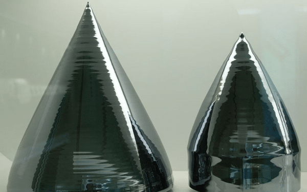
Stage 1: Making Ingots
In order to use silicon extracted from sand as a semiconductor material, it first needs to go through a purification process to increase its purity. The silicon raw material is melted at high temperature to create a high-purity silicon melt, which is then crystallized and solidified. The silicon pillars formed in this way are called ingots. The ingots used in semiconductors are ultra-high-purity silicon ingots using a micro-process of several nanometers (nm).
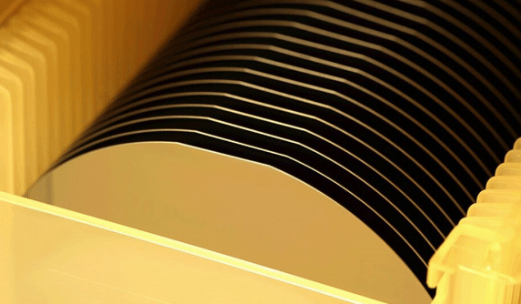
The second stage: cutting the ingot into thin wafers (Wafer Slicing)
In order to make a circular gyro-shaped mirror into a disc-shaped wafer, it needs to be cut into thin slices of uniform thickness using a diamond saw. The diameter of the flake determines the size of the wafer. Wafer sizes include 150mm (6 inches), 200mm (8 inches), 300mm (12 inches), etc. The thinner the wafer, the lower the manufacturing cost, and the larger the diameter, the greater the number of semiconductor chips that can be produced at one time. Therefore, the thickness and size of the wafer are gradually thinning and expanding.
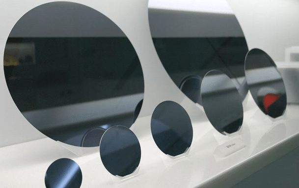
The third stage: Wafer surface polishing (Lapping & Polishing)
The cut wafers need to be processed to make them as smooth as a mirror. This is because the surface of the newly cut wafer is defective and rough, which may affect the precision of the circuit. Therefore, polishing fluid and polishing equipment need to be used to grind the wafer surface smooth. The wafer before processing is like being without clothes, so it is called bare wafer. After multiple stages of physical and chemical processing, IC can be formed on the surface. After the processing stage, it will become the following shape.
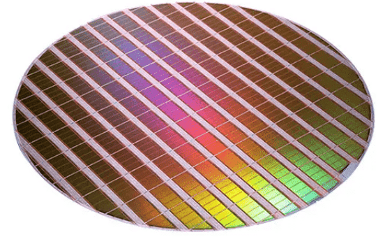
The names of semiconductor wafers are as follows:
1.Wafer: Wafer is the core material of semiconductor integrated circuits and is a round plate.
2.Die: Many quadrilaterals are gathered on a round wafer. These quadrilaterals are IC chips that are integrated electronic circuits.
3.Scribe Line:It seems that the individual grains are stuck together, but in fact there is a certain gap between the grains. This gap is called the dividing line. The purpose of setting up dividing lines between wafers is to cut these wafers one by one and then assemble them into chips after the wafer processing is completed. It is also to leave space for cutting with a diamond saw.
4.Flat Zone:The flat zone is an area created to distinguish the wafer structure and is the standard line for wafer processing. Since the crystal structure of the wafer is very fine and cannot be judged with the naked eye, this flat area is used as the standard to judge the vertical and horizontal position of the wafer.
5.Groove (Notch): Nowadays, wafers with grooves also appear. Compared with flat area wafers, grooved wafers can produce more dies and are therefore very efficient.
The semiconductor industry includes the wafer industry that produces wafers and the wafer processing industry that designs and manufactures wafers as materials. In addition, there is the assembly industry, which cuts processed wafers into die and packages them to protect them from moisture or pressure.
Vacuum pumps are used in many aspects of wafer processing. When the semiconductor industry first started, there were only two processing processes that required the use of vacuum chambers. One is an evaporated aluminum process with only one layer of metal, and the other is to evaporate gold on the back of the silicon wafer to fix the circuit chip on its shell. The vacuum process at that time was performed in a cavity similar to a bell jar. Currently, many chemical reactions in semiconductor manufacturing processes are performed under vacuum conditions, using process chambers to achieve a controlled vacuum environment. Since the late 1980s, process chambers have been constructed as multi-cavity integrated devices. Silicon wafers are transferred from one process chamber to another in a vacuum environment, avoiding the original oxidation of the silicon wafers and reducing contamination.
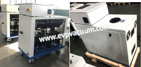
Case: Customer’s application of liquid ring pump system in semiconductor wafer manufacturing, using DLV-1200 and DLV-800 two-stage vacuum pump systems:

The semiconductor industry is a very important application field for vacuum pumps and is currently the main growth driver. At present, vacuum pumps have been widely used in many process links of semiconductor manufacturing, including etching, coating, diffusion, etc. In order to control the manufacturing process at smaller dimensions, there is an increasing need to perform more semiconductor manufacturing process steps with higher precision and uniformity. To achieve this, semiconductor processes must operate in extremely controlled vacuum environments. As functionality and circuit size decrease, the number of process steps in semiconductor manufacturing will continue to increase, resulting in increased demand for vacuum equipment. In addition, miniaturization also requires new manufacturing technologies, such as multi-mode and EUV lithography, which will further drive the adoption of vacuum systems by semiconductor manufacturers.
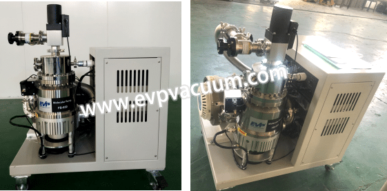
The main types of vacuum pumps used in semiconductor manufacturing include dry vacuum pumps and turbomolecular pumps. Compared with dry pump equipment, in addition to improving speed, process repeatability, flexibility and productivity, it can also significantly save operating costs, maintenance costs and installation space. The key advantages of dry pump equipment, such as dry screw vacuum pump+ roots booster pump unit, turbo molecular pump+scroll dry pump unit;
No water or oil is used for sealing or lubrication of the vacuum stage, making the equipment very economical to run and allowing the user to optimize the vacuum process. In addition, dry pumps eliminate the risk of process contamination or oil carryover into the exhaust treatment system; they do not create waste or contaminate valuable solvents, products or the environment.
Dry scroll vacuum pumps + turbomolecular pumps are usually used in etching and thin film deposition equipment to pump the atmosphere to a certain vacuum to meet the needs of the process. Due to the limited vacuuming capacity of the dry vacuum scroll, a turbomolecular pump is required to evacuate the environment to a high vacuum.
For example, a wafer fab with a monthly output of 40,000 wafers requires 1,000 emission reduction systems, approximately 2,000 dry pumps, and at least 500 turbomolecular pumps. Dry scroll vacuum pumps and abatement systems are sold directly to foundries and integrated equipment manufacturers for use in their manufacturing processes, and turbomolecular pumps are sold directly to equipment manufacturers for integration into their process tools.
At present, EVP’s vacuum products are widely used in the semiconductor industry, and the products meet the needs of the industry. EVP vacuum pumps can be used in cleaning or harsh processes such as crystal pulling, LL, Etching, CVD, ALD, packaging, testing, etc. in the semiconductor industry.
Vacuum pumps are mainly used in the photovoltaic industry, semiconductor industry, new energy industry, etc., with the highest proportion used in the photovoltaic industry, among which the main ones are the crystal pulling process of photovoltaic silicon wafers and the cell process. For more information, please contact Shanghai Kan Special Vacuum Technology Co., Ltd.